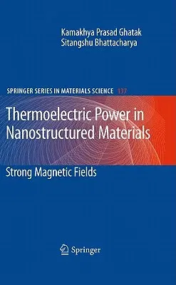
Kamakhya Prasad Ghatak
(Author)Thermoelectric Power in Nanostructured Materials: Strong Magnetic Fields (2010)Hardcover - 2010, 31 July 2010

Qty
1
Turbo
Ships in 2 - 3 days
In Stock
Free Delivery
Cash on Delivery
15 Days
Free Returns
Secure Checkout

Part of Series
Springer Materials Science
Part of Series
Springer Series in Materials Science
Part of Series
Springer Series in Materials Science Springer Series in Mate
Print Length
393 pages
Language
English
Publisher
Springer
Date Published
31 Jul 2010
ISBN-10
364210570X
ISBN-13
9783642105708
Description
Product Details
Book Edition:
2010
Book Format:
Hardcover
Country of Origin:
NL
Date Published:
31 July 2010
Dimensions:
23.37 x
16 x
2.79 cm
ISBN-10:
364210570X
ISBN-13:
9783642105708
Language:
English
Location:
Berlin, Heidelberg
Pages:
393
Publisher:
Series:
Weight:
703.07 gm