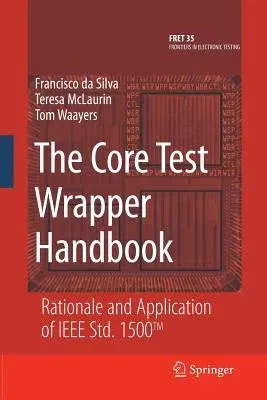
Francisco Da Silva
(Author)The Core Test Wrapper Handbook: Rationale and Application of IEEE Std. 1500(tm) (2006)Paperback - 2006, 20 October 2014

Qty
1
Turbo
Ships in 2 - 3 days
In Stock
Free Delivery
Cash on Delivery
15 Days
Free Returns
Secure Checkout
Part of Series
Frontiers in Electronic Testing
Print Length
276 pages
Language
English
Publisher
Springer
Date Published
20 Oct 2014
ISBN-10
148998769X
ISBN-13
9781489987693
Description
Product Details
Book Edition:
2006
Book Format:
Paperback
Country of Origin:
NL
Date Published:
20 October 2014
Dimensions:
23.39 x
15.6 x
1.65 cm
ISBN-10:
148998769X
ISBN-13:
9781489987693
Language:
English
Location:
New York, NY
Pages:
276
Publisher:
Weight:
435.45 gm

