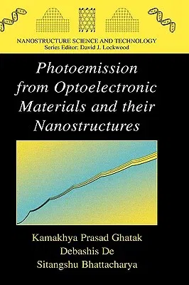
Kamakhya Prasad Ghatak
(Author)Photoemission from Optoelectronic Materials and Their Nanostructures (2009)Hardcover - 2009, 1 July 2009

Qty
1
Turbo
Ships in 2 - 3 days
In Stock
Free Delivery
Cash on Delivery
15 Days
Free Returns
Secure Checkout

Part of Series
Nanostructure Science and Technology
Part of Series
Statistics in Practice
Print Length
329 pages
Language
English
Publisher
Springer
Date Published
1 Jul 2009
ISBN-10
0387786058
ISBN-13
9780387786056
Description
Product Details
Book Edition:
2009
Book Format:
Hardcover
Country of Origin:
NL
Date Published:
1 July 2009
Dimensions:
23.39 x
15.6 x
2.06 cm
Genre:
Nanotechnology
ISBN-10:
0387786058
ISBN-13:
9780387786056
Language:
English
Location:
New York, NY
Pages:
329
Publisher:
Weight:
666.78 gm