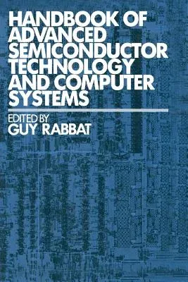
Guy Rabbat
(Author)Handbook of Advanced Semiconductor Technology and Computer Systems (Softcover Reprint of the Original 1st 1988)Paperback - Softcover Reprint of the Original 1st 1988, 24 June 2012

Qty
1
Turbo
Ships in 2 - 3 days
In Stock
Free Delivery
Cash on Delivery
15 Days
Free Returns
Secure Checkout
Part of Series
Van Nostrand Reinhold Electrical/Computer Science and Engine
Print Length
942 pages
Language
English
Publisher
Springer
Date Published
24 Jun 2012
ISBN-10
9401170584
ISBN-13
9789401170581
Description
Product Details
Author:
Book Edition:
Softcover Reprint of the Original 1st 1988
Book Format:
Paperback
Country of Origin:
NL
Date Published:
24 June 2012
Dimensions:
23.39 x
15.6 x
4.83 cm
ISBN-10:
9401170584
ISBN-13:
9789401170581
Language:
English
Location:
Dordrecht
Pages:
942
Publisher:
Weight:
1319.95 gm

