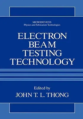
Electron Beam Testing Technology (1993)Hardcover - 1993, 31 July 1993

Qty
1
Turbo
Ships in 2 - 3 days
In Stock
Free Delivery
Cash on Delivery
15 Days
Free Returns
Secure Checkout

Part of Series
Microdevices
Part of Series
Environmental Science Research
Part of Series
Microdevices: Physics and Fabrication Technologies
Print Length
462 pages
Language
English
Publisher
Springer
Date Published
31 Jul 1993
ISBN-10
0306443600
ISBN-13
9780306443602
Description
Product Details
Book Edition:
1993
Book Format:
Hardcover
Country of Origin:
US
Date Published:
31 July 1993
Dimensions:
25.4 x
17.78 x
2.69 cm
ISBN-10:
0306443600
ISBN-13:
9780306443602
Language:
English
Location:
New York, NY
Pages:
462
Publisher:
Weight:
1052.33 gm